At ISSCC 2026, Renesas announced a slew of new technologies for automotive SoCs, including three new SoC technologies for automotive multi-domain electronic control units (ECUs) in software-defined vehicle (SDV) architectures and a configurable 3-nm ternary content-addressable memory (TCAM) architecture designed for automotive SoCs.
Renesas announced its bolstered automotive portfolio at ISSCC.
The releases provide insight into Renesas’s vision for the future—with a common thread of centralized compute, heterogeneous integration, and memory architectures optimized for performance and ISO 26262 compliance
Chiplet Architectures for Multi-Domain Automotive ECUs
Renesas’s first announcement at ISSCC revealed three SoC technologies intended for high-performance automotive multi-domain ECUs. These chips must simultaneously execute heterogeneous workloads while maintaining ASIL D compliance across increasingly complex silicon.
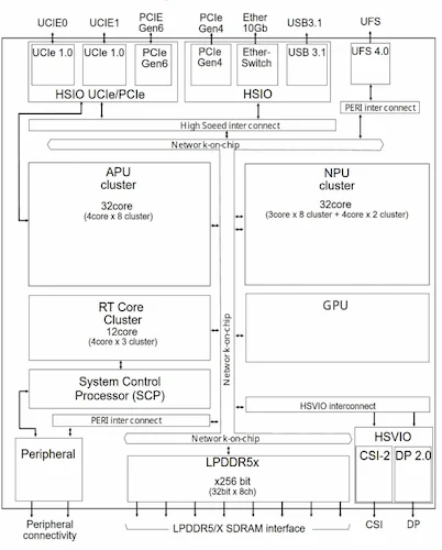
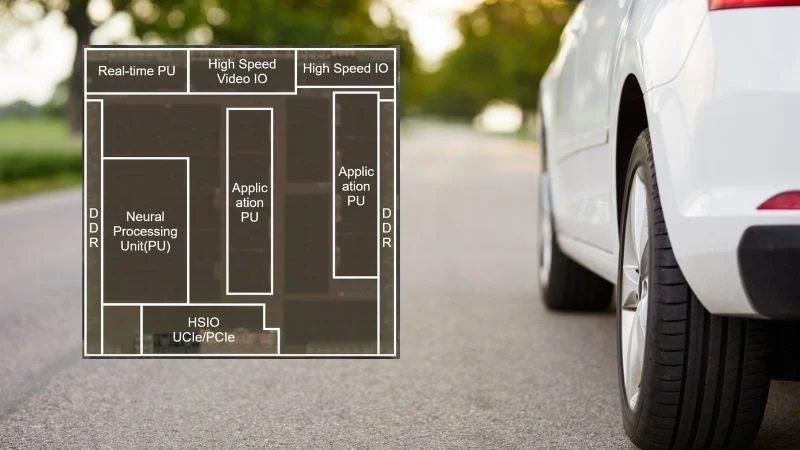
Renesas’s automotive SoC functional block diagram.
The company implemented the following techniques in the R-Car X5H devices for automotive multi-domain ECUs.
Improving UCIe
To support scalable integration, Renesas developed a proprietary chiplet architecture that combines a standard UCIe die-to-die interface with a RegionID-based access control mechanism. Conventional UCIe implementations do not transmit region identifiers across dies. In contrast, Renesas maps RegionIDs into physical address space, encodes them into the UCIe region, and transfers them between chiplets. This allows memory management units and real-time cores to enforce safe access control across dies and to achieve Freedom from Interference (FFI) for functional safety. According to Renesas, its testing confirmed that the UCIe interface supports 51.2 GB/s transfer speeds.
Clock Architectures for NPUs
The second development addresses the growth of neural processing units (NPUs) in advanced automotive SoCs. NPU area has expanded by roughly 1.5x over previous generations, increasing clock latency between shared clock sources and distributed circuits. Renesas aims to solve this issue by redesigning the clock architecture to partition clock pulse generators (CPGs) from module-level blocks into sub-module mini-CPGs (mCPGs). This configuration reduces clock latency and satisfies timing requirements for large AI accelerators.
To maintain zero-defect automotive quality, Renesas integrated test circuits into the hierarchical CPG structure and unified signal paths for user and test clocks. In test mode, upper- and lower-level mCPGs synchronize to a single clock source, enabling unified phase adjustment. In turn, the architecture mitigates synchronization complexity introduced by multi-layer clock generation.
Expanding the Power Domain
The third technology focuses on power efficiency and safety. The SoC incorporates more than 90 power domains with fine-grained power gating to control consumption from milliwatts to tens of watts, depending on workload. Renesas divides power switches into ring and row structures. During power-up, ring switches suppress inrush current, while row switches equalize domain impedance. This arrangement reduces IR drop by approximately 13% compared to conventional designs.
For safety, the SoC uses dual-core lockstep (DCLS) configurations with independent power switches and controllers for the master and checker cores. Loopback monitoring of each power switch gate signal detects OFF-state failures. A temperature-drift-resistant digital voltage monitor improves aging tolerance by 1.4 mV.
Configurable 3-nm TCAM for Automotive SoCs
In a separate announcement, Renesas detailed a configurable 3-nm TCAM architecture designed to extend TCAM use beyond networking into automotive-grade SoCs.
The design combines hard macros with compiler-supported soft-macro auto-generation, with the former supporting search key widths from 8 to 64 bits and entry depths from 32 to 128. Designers can combine these blocks to create large configurations such as 256-bit x 4,096 entries within a single macro. This approach achieves a reported density of 5.27 Mb/mm2.
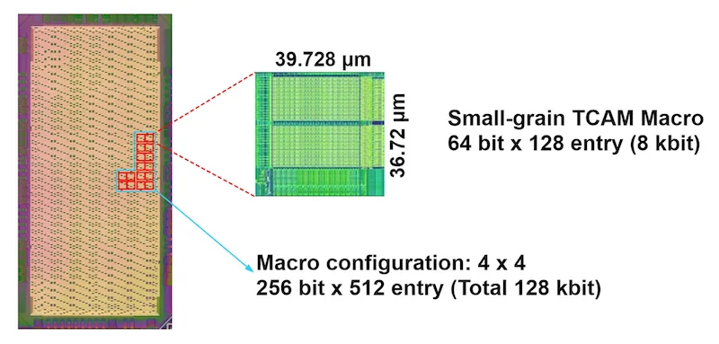
Renesas’s 3-nm TCAM test chip.
To reduce search energy, each hard macro integrates an all-mismatch detection circuit and implements a two-stage pipelined search. After the first stage determines whether all entries are mismatches, the second stage either proceeds or halts. In 64–256-bit x 512-entry configurations, this method reduces search energy by up to 71.1% with column-wise pipelined search for keys larger than 64 bits and up to 65.3% with row-wise pipelined search for keys of 64 bits or less. In a 256-bit x 512-entry implementation, the TCAM achieves 0.167 fJ/bit search energy at a 1.7 GHz clock, for a figure of merit of 53.8.
Renesas also included functional safety enhancements to challenge the limitations of conventional SECDED ECC. Because TCAM bitcells at the same address are physically adjacent, double-bit soft errors cannot historically be corrected. Renesas mitigates this by splitting odd and even data buses to increase physical separation between user data and parity bits, thereby converting potential double-bit errors into correctable single-bit events. A dedicated SRAM for ECC parity, with an independent address decoder, improves the detectability of incorrect-address writes.
Centralized Compute Demands and Architectural Change
Both technologies are now entering productization through devices such as the R-Car X5H, with broader automotive deployment expected as 3-nm manufacturing matures.
All images used courtesy of Renesas.