Researchers are tackling key 6G challenges—from ultra-fast photonic AI for real-time RF processing to novel GaN amplifier behavior and ultra-compact phased-array packaging.
Researchers are racing to deploy 6G with clear goals in mind: speeds exceeding one Tbps, sub-millisecond latencies, AI-native architectures, and seamless integration across the physical and digital worlds. Yet the technical barriers are immense. Spectrum scarcity, thermal constraints, RF front-end inefficiencies, and a need for miniaturized, high-gain antennas threaten to bottleneck progress.
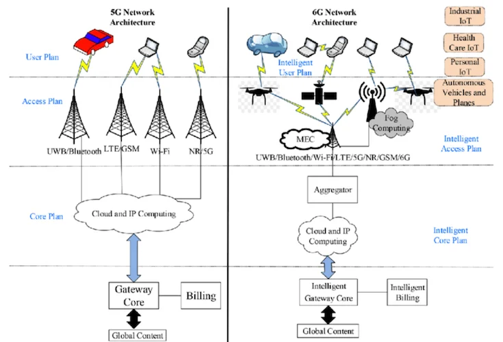
A comparison of 5G and 6G networks. Image used courtesy of Syed Ali Hassan via ResearchGate
This roundup highlights three university-led research efforts that target foundational problems in 6G design, focusing on the intersection of speed, efficiency, and scale. Whether by rethinking photonic processing, exploiting novel RF phenomena in semiconductors, or compressing entire beamforming systems into millimeter-scale modules, each team brings a new layer of feasibility to the 6G vision.
MIT Demonstrates Photonic AI Processor
MIT researchers have developed a photonic deep learning processor. Named MAFT-ONN (Multiplicative Analog Frequency Transform Optical Neural Network), it performs fully analog deep learning directly on raw radio frequency (RF) signals. As 6G systems edge toward terabit-per-second data rates, digital bottlenecks in RF front ends present a major hurdle. The MAFT-ONN system sidesteps this by combining frequency-domain encoding, photoelectric multiplication, and electro-optic nonlinearities to enable real-time, low-latency signal classification and spectrum analysis.
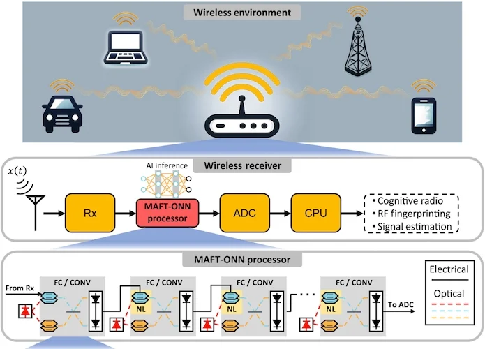
An overview of the MAFT-ONN architecture. Image used courtesy of MIT News
According to the MIT team, the device demonstrated 95% accuracy for RF modulation classification and handled nearly four million analog operations during MNIST digit classification. It also significantly outperformed digital counterparts in latency due to its analog pipeline design. The system paves the way for in-situ AI inference at the RF front end, an increasingly vital capability for 6G applications, such as cognitive radio and adaptive spectrum access.
Crucially, the MIT team’s approach tackles one of 6G’s most pressing problems: bridging AI and RF hardware without incurring the performance penalties of digitization and memory bottlenecks.
University of Bristol Explores GaN Latching
At the University of Bristol in the U.K., researchers have uncovered a novel phenomenon in superlattice castellated field-effect transistors (SLCFETs): a form of reversible, sub-60 mV/decade latching triggered by localized impact ionization. Built using multi-channel GaN structures with up to 1,000 fins, the devices demonstrate steep subthreshold slopes and broad transconductance characteristics, features that could enable more linear and efficient RF power amplifiers for 6G systems.
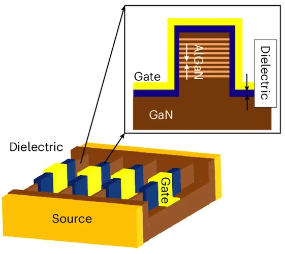
Schematics of a portion of a SLCFET. Image used courtesy of the University of Bristol
The research, conducted in collaboration with Northrop Grumman, suggests that this latching effect, previously believed to be detrimental, is non-degrading and potentially beneficial. It enhances linearity and allows wider voltage swings, thereby increasing output power.
With 6G operating at higher frequencies and on tighter power budgets, Bristol’s work offers a potential route to boosting RF performance without increasing device size. Their modeling, backed by SEM imaging and electroluminescence, also provides a blueprint for managing fin-width variability during fabrication.
Tokyo Scientists Miniaturize Phased-Array Transceivers
At the Institute of Science, Tokyo, researchers have fabricated an ultra-compact 6G phased-array transceiver leveraging a custom 3D packaging platform known as X-Architecture. Targeting sub-terahertz frequencies (specifically around 140 GHz), the module integrates four-channel beamforming in a footprint smaller than a coin. This marks a key milestone in developing miniaturized, directional mmWave radios for 6G mobile devices and wearables.
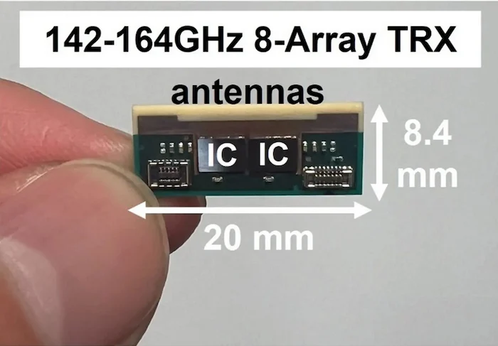
The Tokyo team’s compact 20 mm × 8.4 mm transceiver module operates in the 142–164-GHz band. Image used courtesy of the Institute of Science, Tokyo
The transceiver’s four stacked dies integrate silicon ICs for RF, baseband, and control, bonded using through-silicon vias and micro-bump interconnects. Despite its size, the device achieves beam steering, high gain, and low error vector magnitude, making it suitable for ultra-reliable, high-speed data links.
Unlike many 6G demonstrations, which are often constrained to lab setups, Tokyo’s prototype emphasizes real-world feasibility by combining high integration density with robust thermal and RF performance. This research directly addresses one of 6G’s key barriers: implementing phased-array technologies at form factors compatible with consumer electronics.