Advanced process nodes do not become useful on manufacturing capability alone. Designers also need tools compatible with the node, IP validated against it, and flows that can take a design from architecture to signoff without turning every step into custom work. Siemens, Cadence, Synopsys, and Keysight have each announced expanded support for Intel 14A, with several also covering Intel 18A-P.
Intel 14A ecosystem certifications are helping chip designers prepare tools, flows, IP, and simulation support for next-generation semiconductor designs. Image used courtesy of Siemens
The updates give design teams a clearer path into Intel’s next-generation process technologies, especially for AI, HPC, mobile, RF, and multi-die designs.
Siemens Extends Verification and Packaging Support
Siemens certified its Calibre nmPlatform and Solido Simulation Suite for Intel 14A and Intel 18A-P process technologies. That includes Calibre tools for design rule checking, layout versus schematic verification, reliability checks, and yield enhancement. On the simulation side, Solido SPICE and Analog FastSPICE are certified as well.
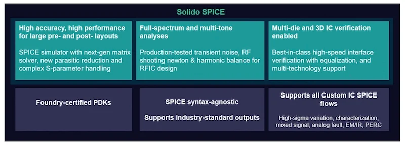
Solido SPICE, part of Siemens' Solido Simulation Suite. Image used courtesy of Siemens
The update is not only about basic process support. Siemens also enabled Solido tools with Open Model Interface for aging modeling and reliability analysis. Analog FastSPICE is enabled through Intel’s Custom Reference Flow, which gives analog and mixed-signal designers a more direct route through simulation and verification.
Siemens and Intel also collaborated on a workflow for advanced packaging technologies, including EMIB and EMIB-T with through silicon vias. That matters as more designs move toward chiplet architectures rather than single-die scaling. For designers, the value is confidence. They can keep using familiar verification and simulation tools while targeting newer Intel processes and packaging options.
Cadence Certifies AI-Driven Reference Flows
Cadence certified its AI-driven digital and custom reference flows, tools, and solutions for Intel 18A-P and Intel 14A. The flows are based on the latest Intel Foundry process design kits and cover implementation, verification, physical signoff, reliability verification, timing and power signoff, and analog/custom design.
Cadence is also tying the announcement to its broader collaboration with Intel. The companies previously expanded design IP optimized for Intel 18A and 18A-P and signed a multi-year design technology co-optimization agreement targeting Intel 14A. 14A is not just another node migration. It brings technologies such as RibbonFET 2 and PowerDirect, which affect how tools need to handle power, performance, routing, and reliability.
Cadence and Intel also developed an advanced packaging reference flow for EMIB and EMIB-T. The goal is to reduce data conversion steps, support concurrent design work, and give designers earlier insight into thermal, signal integrity, and power integrity issues across dies and packages. Cadence also points to silicon-validated IP test chips on Intel 18A using its interface and memory IP. That gives customers more confidence that Cadence IP and flows can carry forward across Intel’s advanced nodes.
Synopsys Pushes From DTCO to System-Aware Co-Design
Synopsys announced certified AI-powered EDA flows for Intel 14A, building on its certified and production-ready tools and IP for Intel 18A and Intel 18A-P.
Its announcement leans heavily into system-level design. At angstrom-scale geometries, especially with backside power delivery and dense integration, electrical, thermal, and electromagnetic effects become harder to separate. Synopsys is addressing that with certified implementation and signoff flows connected to multiphysics analysis for power integrity, thermal behavior, and electromagnetic effects.
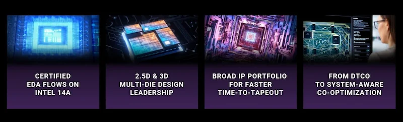
Synopsys certified AI-powered EDA flows, multiphysics analysis, IP, and multi-die design support for Intel 14A. Image used courtesy of Synopsys
The company is also extending its multi-die support through 3DIC Compiler for Intel EMIB and EMIB-T. That includes early bump and TSV planning, automated UCIe and HBM routing, and analysis across dies, interconnect, and package. Synopsys also highlighted IP for Intel 14A, including PCIe 7.0, 224G SerDes, USB 4, eUSB, embedded memories, logic libraries, and IOs. That is important because IP availability can be just as critical as tool certification. Designers do not want to build every interface block from scratch at a new node.
Keysight Certifies RFPro for EM Simulation
Keysight’s update is more focused, but still important. The company certified RFPro electromagnetic design software, part of Keysight ADS, for Intel 14A and Intel 18A-P. That gives RFIC and mixed-signal designers a validated EM simulation path before tapeout. At advanced nodes, a mismatch between electromagnetic behavior and circuit behavior can turn into an expensive redesign.
Keysight’s announcement builds on earlier collaboration with Intel Foundry, including support for Intel 18A and EMIB-T advanced packaging.
Why the Certifications Matter
Together, these announcements make Intel 14A feel less like an isolated process milestone and more like a usable design platform. Siemens strengthens verification and packaging workflows. Cadence brings certified AI-driven implementation and custom flows with advanced packaging support. Synopsys adds system-aware co-design, multiphysics analysis, and broad IP. Keysight gives RF and mixed-signal teams a certified EM path.
For designers, that reduces the uncertainty that usually comes with adopting a new node. The tools, flows, simulation models, packaging support, and IP are being lined up before design teams commit their largest projects. That is the real point. Intel 14A adoption will depend not only on transistor technology, but on whether customers can get from idea to working silicon without rebuilding the design path themselves.