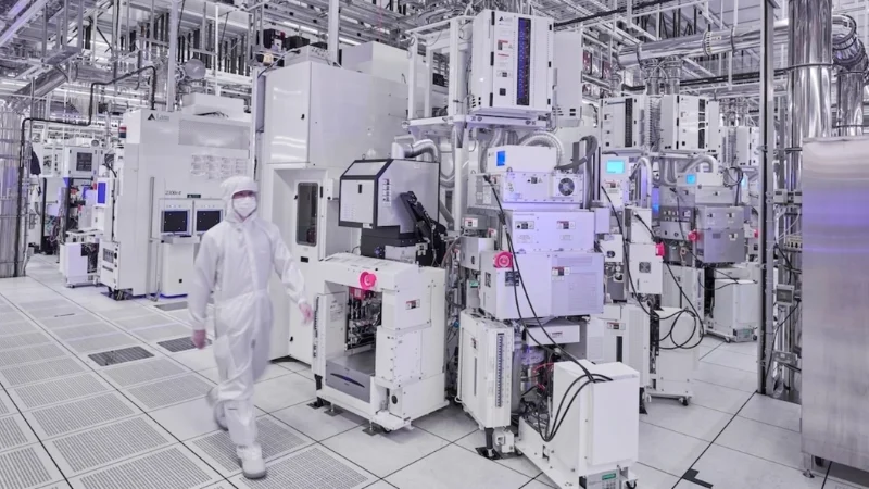

Chip scaling has been running into a hard wall for years. Transistors keep shrinking, but the old method of simply packing more devices side by side is getting harder to sustain. At some point, there just is not enough room left in two dimensions. IBM is trying to move around that problem by building upward in a new way.
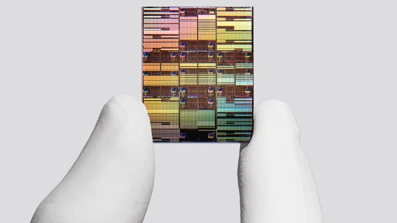
IBM’s sub-1 nm chip technology uses a new nanostack architecture to increase transistor density and push logic scaling into the angstrom era.
The company has introduced what it calls the world’s first sub-1 nanometer chip technology, built around a new 3D transistor architecture called nanostack. The design targets the 0.7-nm node, also described as 7 angstroms, and IBM says it can pack nearly 100 billion transistors onto a chip about the size of a fingernail. But the chip is not just smaller because IBM pushed existing transistor structures further. It is smaller because the company completely changed the geometry of transistor arrangement.
What Is Nanostack?
Nanostack builds on IBM’s nanosheet transistor technology, but takes it into three dimensions. Instead of placing n-type and p-type transistors side by side on the same plane, IBM’s architecture stacks and staggers them vertically. That matters because chipmakers have spent decades scaling along the X and Y axes. Nanostack adds the Z axis. In simple terms, it gives designers another direction to use when space on the surface is running out.
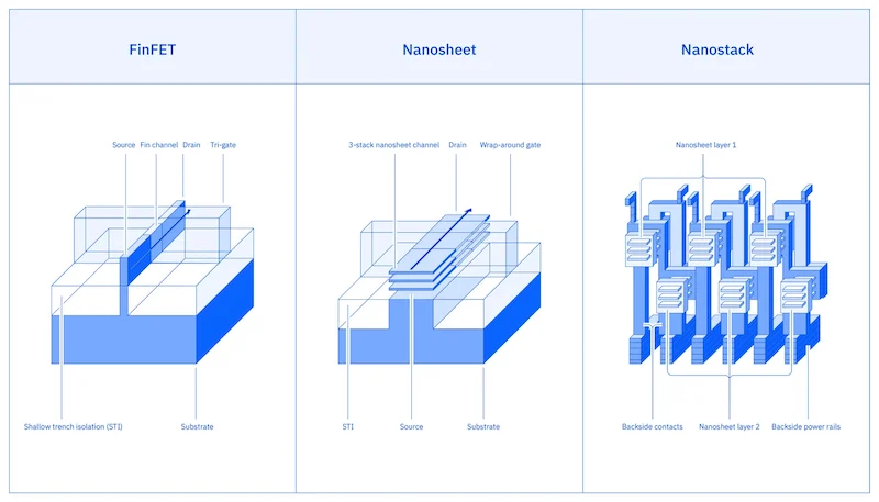
In 2017, IBM developed a nanosheet transistor architecture (center) to replace FinFET technology (left). Now, the company claims nanostack transistor architecture (right) may extend transistor scaling over the next 10 years.
The architecture uses 3D sequential integration and wafer bonding to stack transistor layers. The devices are also staggered rather than stacked in a perfectly vertical column. That brick-like arrangement helps improve density while still allowing the transistors to be connected and controlled.
Another important consideration is material flexibility. By separating n-type and p-type transistors into different layers, IBM can optimize the channel materials for each device type rather than compromise on a single material for both. That can help improve performance and efficiency at extremely small dimensions.
How It Enables Sub-1 nm Scaling
The move below 1 nm is not just about making features smaller. At these dimensions, traditional scaling starts to run into practical limits. Routing power and signals become a challenge. Leakage is harder to manage. SRAM scaling poses a bottleneck. Even small alignment errors can be serious.
IBM’s nanostack approach attacks several of those problems at once. The vertical transistor structure increases density without relying only on lateral shrinking. Thin dielectric wafer bonding allows the stacked layers to connect with low defect levels. Backside power delivery shifts power routing away from the chip's front side, freeing up space for signal routing and improving density.
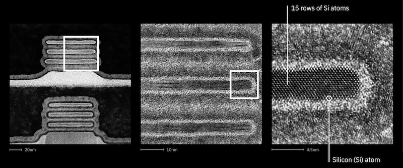
Microscopy images of IBM’s sub-1 nm chip technology show the stacked nanosheet structure used to increase transistor density at near atomic dimensions.
IBM also points to a 40% improvement in SRAM scaling, which is especially important for AI chips. On-chip memory is one of the major bottlenecks in AI workloads. More dense SRAM can help feed compute units faster and reduce the amount of data that needs to move off-chip. High NA EUV lithography is another piece of the path forward. It enables finer circuit patterns to be printed with fewer process steps, reducing defects and improving yield as wires and transistor structures continue to shrink.
Why IBM Is Calling It the Smallest and Most Powerful
IBM’s claim is big, but the company does provide several technical markers to back it up.
The 0.7-nm node is positioned below the 1-nm threshold and ahead of IBM’s earlier 2-nm technology. The new chip is projected to reach nearly twice the transistor density of IBM’s 2-nm node. IBM also projects up to 50% higher performance or 70% better energy efficiency compared with its 2-nm technology. For AI accelerators, IBM researchers estimate that chips built with 7 angstrom technology could reach around 9,000 TOPS, compared with roughly 1,500 TOPS for many current AI accelerators.
IBM says the architecture has moved beyond concept. The company reports experimental validation through ultra-thin dielectric bonding, dual-channel engineering, and functional CMOS inverter operation.
Where It Could Matter Most
The most obvious application is AI. However, mobile and laptop devices could also benefit if the technology does reach commercial production. More efficient chips could potentially mean longer battery life or higher performance in the same power envelope.
IBM also points toward autonomous systems, monitoring devices, advanced electronics, communication infrastructure, and future computing platforms. Really, any system that needs more compute in less space could benefit. The company sees a possible path to production within about five years.
All images used courtesy of IBM.