Rohm Scales Production on 650 V GaN HEMTs
In partnership with Ancora Semiconductors, Rohm is sending two of its GaN transistors into mass production.
Gallium nitride (GaN) has taken massive strides from idea to commercialized product in the past decade. While GaN products still don’t have the supply chain and manufacturing capabilities that silicon products have, there are many in the industry looking to further build out the GaN infrastructure.
This week, Rohm Semiconductor announced that in collaboration with Ancora Semiconductors, two of its GaN products are headed to mass production. In this article, we’ll compare current GaN and silicon technologies and discuss Rohm’s 650 V GaN high-electron-mobility transistors (HEMTs). Rohm's 650 V GaN HEMTs.
GaN vs. Silicon: Breakdown Voltage
Because of its unique material properties, GaN-based transistors offer a number of key advantages over silicon-based transistors.
One of these key advantages is that GaN FETs experience a much higher breakdown voltage than silicon FETs. In a semiconductor, the bandgap of a material defines the energy difference between the highest energy level in the valence band and the lowest energy level in the conductance band. In other words, the bandgap determines the amount of energy that is required to excite an electron from the valence band to the conduction band.
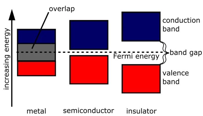
Semiconductor bandgap.
GaN has a much larger bandgap (3.2 eV) than that of silicon (1.1 eV). The practical result of this difference is that it requires significantly more energy to excite an electron in a GaN substrate than in a silicon substrate. In terms of transistors, this means that GaN can offer significantly higher breakdown voltages (in other words, the amount of voltage it can withstand before getting damaged) than silicon.
For this reason, GaN has become extremely popular in power electronics, where high voltages are necessary. In fact, GaN has a breakdown field of 3.3 MV/cm, while silicon has a breakdown field of 0.3 MV/cm—which is a 10x difference.
GaN vs. Silicon: Efficiency
Beyond breakdown voltage, GaN also has the advantage of power efficiency compared to silicon.
GaN has much higher electron mobility than silicon, meaning that electrons can conduct more freely through GaN than silicon. In the context of a transistor, this means that GaN FETs have a lower RDS(on) than a silicon transistor. This directly results in lower I2*R losses while the FET is conducting, making GaN FETs more power efficient during conduction.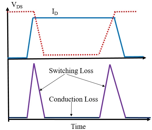
Switching loss and conduction loss in a transistor.
Additionally, GaN transistors have better switching characteristics than their silicon counterparts. Specifically, the greater electron mobility and decreased parasitic capacitance of GaN FETs allow for faster switching frequencies. With faster-switching frequencies, the transistor will spend less time in the linear region, which is where most switching losses occur.
GaN FETs' efficiency makes them useful in power electronics, where losses are potentially great and thermal management is a key issue.
Rohm Scales 650 V GaN HEMTs
This week, Rohm announced that two of its GaN HEMT offerings have reached mass production. The GNP1070TC-Z and the GNP1150TCA-Z are similar offerings, with both offering breakdown voltages of 650 V and targeting power applications.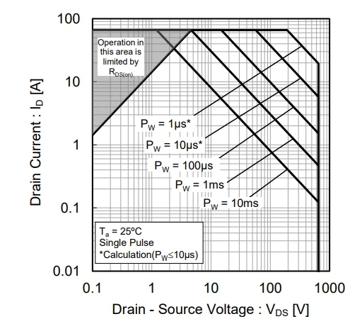
GNP1070TC-Z drain current vs. VDS.
Along with a 650 V VDss, the GNP1070TC-Z offers a typical RDS(on) of 70 mΩ, a gate charge of 5.2 nC, and a maximum continuous drain current of 20 A. The GNP1150TCA-Z, on the other hand, has an RDS(on) of 150 mΩ, a gate charge of 2.7 nC, and a maximum continuous drain current of 11 A.
This news comes on the heels of Rohm’s recent announcement of its 150 V GaN HEMTs also reaching mass production in March of this year.